AArch64 option ROMs for AMD GPUs

Usually, on AArch64 systems with proprietary UEFI firmware, a HDMI/DP display does not light up until the point where the OS driver takes control. This makes it tedious to access the UEFI configuration menus or the GRUB bootloader menu, since it either requires connecting a VGA monitor to the BMC, or finding it on the network and connecting to it.

Also, OS drivers for GPUs are all developed and tested under the assumption that the option ROM driver has executed when the OS takes over. This means any errata handling or OEM tweaks may not take effect as they would otherwise.

For AMD cards, it is possible to address this problem by replacing the x86 EFI driver on the card with an AArch64 one (or adding one if only a legacy x86 driver was there in the first place)

  1. Build flashrom from the ati branch at https://github.com/ardbiesheuvel/flashrom
  2. Check out edk2 (https://github.com/tianocore/edk2) and build the base tools (make -C BaseTools/)
  3. Dump the option ROM (as root)

    # ./flashrom -p ati_spi -r vbios.rom

    (Note that the ati_spi driver is currently hardcoded to support PCI domain/segment #0 only. )

  4. List the table of contents
    $ edk2/BaseTools/Source/C/bin/EfiRom -d vbios.rom 
    Image 1 -- Offset 0x0
      ROM header contents
        Signature              0xAA55
        PCIR offset            0x0244
        Signature               PCIR
        Vendor ID               0x1002
        Device ID               0x67DF
        Length                  0x0018
        Revision                0x0000
        DeviceListOffset        0x00
        Class Code              0x030000
        Image size              0xEA00
        Code revision:          0x0F32
        MaxRuntimeImageLength   0x00
        ConfigUtilityCodeHeaderOffset 0x4D41
        DMTFCLPEntryPointOffset 0x2044
        Indicator               0x00
        Code type               0x00
    Image 2 -- Offset 0xEA00
      ROM header contents
        Signature              0xAA55
        PCIR offset            0x001C
        Signature               PCIR
        Vendor ID               0x1002
        Device ID               0x67DF
        Length                  0x0018
        Revision                0x0000
        DeviceListOffset        0x00
        Class Code              0x030000
        Image size              0xE600
        Code revision:          0x0000
        MaxRuntimeImageLength   0x00
        ConfigUtilityCodeHeaderOffset 0x4F47
        DMTFCLPEntryPointOffset 0x2050
        Indicator               0x80   (last image)
        Code type               0x03   (EFI image)
      EFI ROM header contents
        EFI Signature          0x0EF1
        Compression Type       0x0001 (compressed)
        Machine type           0x8664 (X64)
        Subsystem              0x000B (EFI boot service driver)
        EFI image offset       0x0058 (@0xEA58)


    The first image contains the ATOM BIOS code, and should be kept – it is loaded by the OS driver when it probes the card. The second image is the existing x86 EFI driver.

  5. Create a compressed option ROM image from the AMD GOP driver for arm64 (https://www.amd.com/en/support/kb/release-notes/rn-aar), using the vendor and device IDs taken from the output above.
    $ edk2/BaseTools/Source/C/bin/EfiRom -f 0x1002 -i 0x67DF -l 0x030000 -ec Arm64Gop_1_68.efi

    This will create a file called Arm64Gop_1_68.rom in the current directory.

  6. Copy the ROM image to a new file, and store the old one for safe keeping.

  7. If the ROM image has sufficient space for an additional driver and you want to keep the x86 EFI driver, or if it does not have a EFI driver in the first place, you will need to use a hex editor to find the 0x80 ‘indicator’ byte at offset 22 of the last header that starts with PCIR, and change it to 0x0.

  8. Insert the AMD GOP option ROM image into the copy of the option ROM

    $ dd if=Arm64Gop_1_68.rom of=vbios_new.rom conv=notrunc seek=<byte offset>

    where byte offset equals offset + size of the preceding image. Note that this must be a multiple of 512. For the image above, this would be 0xea00 + 0xe600, assuming we are keeping the x86 driver (or 0xea00 if not).

  9. Dump the new image contents to double check that everything looks as expected.
    $ edk2/BaseTools/Source/C/bin/EfiRom -d vbios_new.rom 
    Image 1 -- Offset 0x0
      ROM header contents
        Signature              0xAA55
        PCIR offset            0x0244
        Signature               PCIR
        Vendor ID               0x1002
        Device ID               0x67DF
        Length                  0x0018
        Revision                0x0000
        DeviceListOffset        0x00
        Class Code              0x030000
        Image size              0xEA00
        Code revision:          0x0F32
        MaxRuntimeImageLength   0x00
        ConfigUtilityCodeHeaderOffset 0x4D41
        DMTFCLPEntryPointOffset 0x2044
        Indicator               0x00
        Code type               0x00
    Image 2 -- Offset 0xEA00
      ROM header contents
        Signature              0xAA55
        PCIR offset            0x001C
        Signature               PCIR
        Vendor ID               0x1002
        Device ID               0x67DF
        Length                  0x0018
        Revision                0x0000
        DeviceListOffset        0x00
        Class Code              0x030000
        Image size              0xE600
        Code revision:          0x0000
        MaxRuntimeImageLength   0x00
        ConfigUtilityCodeHeaderOffset 0x4F47
        DMTFCLPEntryPointOffset 0x2050
        Indicator               0x00
        Code type               0x03   (EFI image)
      EFI ROM header contents
        EFI Signature          0x0EF1
        Compression Type       0x0001 (compressed)
        Machine type           0x8664 (X64)
        Subsystem              0x000B (EFI boot service driver)
        EFI image offset       0x0058 (@0xEA58)
    Image 3 -- Offset 0x1D000
      ROM header contents
        Signature              0xAA55
        PCIR offset            0x001C
        Signature               PCIR
        Vendor ID               0x1002
        Device ID               0x67DF
        Length                  0x001C
        Revision                0x0003
        DeviceListOffset        0x00
        Class Code              0x030000
        Image size              0xFA00
        Code revision:          0x0000
        MaxRuntimeImageLength   0x00
        ConfigUtilityCodeHeaderOffset 0x00
        DMTFCLPEntryPointOffset 0x00
        Indicator               0x80   (last image)
        Code type               0x03   (EFI image)
      EFI ROM header contents
        EFI Signature          0x0EF1
        Compression Type       0x0001 (compressed)
        Machine type           0xAA64 (AA64)
        Subsystem              0x000B (EFI boot service driver)
        EFI image offset       0x0038 (@0x1D038)


  10. Use flashrom with the -w switch to write the new image back to the device.
  11. In the UEFI shell, the ‘drivers’ command will list all the UEFI drivers that have been loaded. E.g.,

    D1 00014400 D - -  1  - AMD GOP ARM64 Release Driver, Rev. Offset(0x1D000,...

    where the ‘D’ in the third column signifies that it has attached to the device.

GHASH for high-end ARM cores

After years of using Cortex-A57 or A53 based systems as both my development machines as well as my optimization targets, I was recently given a ThunderX2 workstation, and after having moved my development environment to it, I have started  looking into whether the existing accelerated crypto drivers in the Linux kernel perform optimally on this micro-architecture.

Marvell’s ThunderX2 core (née Broadcom Vulcan) is a server class CPU with a deep pipeline. This typically means that it takes longer for the result of an instruction to become available to subsequent instructions, and instead of stalling the pipeline waiting for that result, we should try to do some other useful work in the meantime.

So for the simpler AES modes such as CBC and CTR, I have increased the interleave factor from 4x to 5x, resulting in a speedup of around 11% on ThunderX2. This result fueled my suspicion that the GCM code, which was using an interleave factor of only 2x, could benefit even more from this approach, and since I already added an implementation of GHASH (one of the constituent parts of GCM) that uses aggregation to operate on 4 blocks of input at a time, it should simply be a matter of combining this code with a 4-way interleaved implementation of CTR.

GHASH aggregation

GHASH is not a general purpose cryptographic hash function, but one that was specifically designed for (and should only be used in) AES in GCM mode. It is based on multiplication in GF(2128), and basically comes down to the following

X[0] = (H * I[0]) mod M
X[1] = (H * (X[0] ^ I[1])) mod M
X[n] = (H * (X[n-1] ^ I[n])) mod M

where I[] is an input array of 16 byte blocks, and the output of the hash function is the last value in the array X[]. H is a quantity that is derived from the AES key by encrypting a single AES block consisting of NUL bytes, and M is GHASH’s characteristic polynomial x128 + x7 + x2 + x + 1 over GF(2128).

Each line involves a multiplication in GF(2128), which means that it consists a multiplication step and a modulo division step, and it is possible the amortize the cost of the latter step over multiple multiplications, increasing performance. For example, we can process two blocks at a time like so

X[n] = (H * (((H * (X[n-2] ^ I[n-1])) mod M) ^ I[n])) mod M
     = ((H^2 * (X[n-2] ^ I[n-1])) ^ (H * I[n])) mod m

This is called GHASH aggregation, and was implemented for the core GHASH transform here. Note that this requires powers of H to be precomputed, and so we cannot apply this transformation an arbitrary number of times.

Another thing to note is that this algorithm combines the highest power of H with the first input block, which means that if we want to reuse the same code sequence to process fewer than n blocks, we need to populate the input blocks from right to left, and jump to the appropriate point in the routine so that only the lower powers of H are used in the computation.

Handling the tail

GCM is an AEAD (Authenticated Encryption with Associated Data) which can operate on inputs of any size. Since GCM is mainly used in the networking space, we should expect having to deal mostly with the typical size of a network packet, which is ~1500 bytes. This means that our 4-way aggregated code operating on 4 blocks or 64 bytes at a time will always have to deal with a tail block of less than 64 bytes in size.

Since out-of-order cores with deep pipelines perform poorly when running code with lots of branches and tight loops that load small quantities at a time, we should try to handle the tail with as few branches as possible, and use large, potentially overlapping loads to get the data into SIMD registers.

This is what the sequence below implements. It unconditionally performs four 16-byte loads, and manipulates the input address and the post-increment values so that we end up with I[] populated right to left with between 1 and 63 bytes of remaining input. (x0 contains the source address, and x2 the size of the remaining input minus 64)

mov     x15, #16
ands    x19, x0, #0xf
csel    x19, x19, x15, ne
adr_l   x17, .Lpermute_table + 16

sub     x11, x15, x19
add     x12, x17, x11
ld1     {T1.16b}, [x12]
sub     x11, x2, x11

cmp     x0, #-16
csel    x14, x15, xzr, gt
cmp     x0, #-32
csel    x15, x15, xzr, gt
cmp     x0, #-48
csel    x16, x19, xzr, gt
csel    x2, x2, x11, gt

ld1     {I0.16b}, [x2], x14
ld1     {I1.16b}, [x2], x15
ld1     {I2.16b}, [x2], x16
ld1     {I3.16b}, [x2]
tbl     I3.16b, {I3.16b}, T1.16b

Since we always load at least 16 bytes, it is up to the caller to present the input in a way that permits doing so if the entire input is less than 16 bytes in size (e.g, by copying the input to the end of a 16 byte buffer)

CTR encryption

While the 4-way GHASH code requires taking another code path through the 4-way routine when it is invoked with less than 4 blocks of input, the CTR code can be modified more easily to support this, by incrementing the overall counter by the remaining number of blocks, and then subtracting 4-n for each keystream block n. This naturally populates the keystream blocks from right to left as well, and instead of using a different encryption routine depending on the remaining input size, we can just unconditionally generate a 64 byte keystream and discard the parts that we don’t need.

Generating the tag

The final step in performing GCM is generating the authentication tag, which involves one final round of GHASH on a block of input containing the input size, and a final pass of CTR encryption.

While the existing code does not handle the tail or the tag directly, and jumps back to C code instead to copy the tail into a stack buffer and process it via the split GHASH and CTR routines, we have now incorporated this into the core GCM transform. This means we can go one step further, and fold the tag generation in as well.

ld1     {INP3.16b}, [x10]             // load lengths[]
mov     w9, #1                        // one block of input
bl      pmull_gcm_ghash_4x

mov     w11, #(0x1 << 24)             // BE '1U'
ld1     {KS0.16b}, [x5]               // load upper counter
mov     KS0.s[3], w11                 // set lower counter

enc_block KS0, x7, x6, x12

ext     X.16b, X.16b, X.16b, #8
rev64   X.16b, X.16b
eor     X.16b, X.16b, KS0.16b
st1     {XL.16b}, [x10]               // store tag

Conclusion

When combining all the changes above, we end up with a routine that can consume the entire encryption input buffer including the tail and the input block for the tag, and process it in a way that is up to 25% faster than the old code for 1500 byte blocks. Note that 4 KiB blocks are only 11-16% faster, and on other micro-architectures, performance regresses slightly for large inputs. This is not a use case worth obsessing about, though. More performance numbers below, the full implementation can be found here.

AES-128 AES-192 AES-256
#bytes 512 1500 4k 512 1500 4k 512 1500 4k
TX2 35% 23% 11% 34% 20% 9% 38% 25% 16%
EMAG 11% 6% 3% 12% 4% 2% 11% 4% 2%
A72 8% 5% -4% 9% 4% -5% 7% 4% -5%
A53 11% 6% -1% 10% 8% -1% 10% 8% -2%

UEFI driver pitfalls and PC-isms

Even though Intel created UEFI (still known by its TLA EFI at the time) for Itanium initially, x86 is by far the dominant architecture when it comes to UEFI deployments in the field, and even though the spec itself is remarkably portable to architectures such as ARM, there are a lot of x86 UEFI drivers out there that cut corners when it comes to spec compliance. There are a couple of reasons for this:

  • the x86 architecture is not as heterogeneous as other architectures, and while the form factor may vary, most implementations are essentially PCs;
  • the way the PC platform organizes its memory and especially its DMA happens to result in a configuration that is rather forgiving when it comes to UEFI spec violations.

UEFI drivers provided by third parties are mostly intended for plugin PCI cards, and are distributed as binary option ROM images. There are very few open source UEFI drivers available (apart from the _HCI class drivers and some drivers for niche hardware available in Tianocore), and even if they were widely available, you would still need to get them into the flash ROM of your particular card, which is not a practice hardware vendors are eager to support.
This means the gap between theory and practice is larger than we would like, and this becomes apparent when trying to run such code on platforms that deviate significantly from a PC.

The theory

As an example, here is some code from the EDK2 EHCI (USB2) host controller driver.

  Status = PciIo->AllocateBuffer (PciIo, AllocateAnyPages,
                     EfiBootServicesData, Pages, &BufHost, 0);
  if (EFI_ERROR (Status)) {
    goto FREE_BITARRAY;
  }

  Bytes = EFI_PAGES_TO_SIZE (Pages);
  Status = PciIo->Map (PciIo, EfiPciIoOperationBusMasterCommonBuffer,
                     BufHost, &Bytes, &MappedAddr, &Mapping);
  if (EFI_ERROR (Status) || (Bytes != EFI_PAGES_TO_SIZE (Pages))) {
    goto FREE_BUFFER;
  }

  ...

  Block->BufHost  = BufHost;
  Block->Buf      = (UINT8 *) ((UINTN) MappedAddr);
  Block->Mapping  = Mapping;

This is a fairly straight-forward way of using UEFI’s PCI DMA API, but there a couple of things to note here:

  • PciIo->Map () may be called with the EfiPciIoOperationBusMasterCommonBuffer mapping type only if the memory was allocated using PciIo->AllocateBuffer ();
  • the physical address returned by PciIo->Map () in MappedAddr may deviate from both the virtual and physical addresses as seen by the CPU (note that UEFI maps VA to PA 1:1);
  • the size of the actual mapping may deviate from the requested size.

However, none of this matters on a PC, since its PCI is cache coherent and 1:1 mapped. So the following code will work just as well:

  Status = gBS->AllocatePages (AllocateAnyPages, EfiBootServicesData,
                  Pages, &BufHost);
  if (EFI_ERROR (Status)) {
    goto FREE_BITARRAY;
  }

  ...

  Block->BufHost  = BufHost;
  Block->Buf      = BufHost;

So let’s look at a couple of ways a non-PC platform can deviate from a PC when it comes to the layout of its physical address space.

DRAM starts at address 0x0

On a PC, DRAM starts at address 0x0, and most of the 32-bit addressable physical region is used for memory. Not only does this mean that inadvertent NULL pointer dereferences from UEFI code may go entirely unnoticed (one example of this is the NVidia GT218 driver), it also means that PCI devices that only support 32-bit DMA (or need a little kick to support more than that) will always be able to work. In fact, most UEFI implementations for x86 explicitly limit PCI DMA to 4 GB, and most UEFI PCI drivers don’t bother to set the mandatory EFI_PCI_IO_ATTRIBUTE_DUAL_ADDRESS_CYCLE attribute for >32 bit DMA capable hardware either.

On ARM systems, the amount of available 32-bit addressable RAM may be much smaller, or it may even be absent entirely. In the latter case, hardware that is only 32-bit DMA capable can only work if a IOMMU is present and wired into the PCI root bridge driver by the platform, or if DRAM is not mapped 1:1 in the PCI address space. But in general, it should be expected that ARM platforms use at least 40 bits of address space for DMA, and that drivers for 64-bit DMA capable peripherals enable this capability in the hardware.

PCI DMA is cache coherent

Although not that common, it is possible and permitted by the UEFI spec for PCI DMA to be non cache coherent. This is completely transparent to the driver, provided that it uses the APIs correctly. For instance, PciIo->AllocateBuffer () will return an uncached buffer in this case, and the Map () and Unmap () methods will perform cache maintenance under the hood to keep the CPU’s and the device’s view of memory in sync. Obviously, this use case breaks spectacularly if you cut corners like in the second example above.

PCI memory is mapped 1:1 with the CPU

On a PC, the two sides of the PCI host bridge are mapped 1:1. As illustrated in the example above, this means you can essentially ignore the device or bus address returned from the PciIo->Map () call, and just program the CPU physical address into the DMA registers/rings/etc. However, non-PC systems may have much more extravagant PCI topologies, and so a compliant driver should use the appropriate APIs to obtain these addresses. Note that this is not limited to inbound memory accesses (DMA) but also applies to outbound accesses, and so a driver should not interpret BAR fields from the PCI config space directly, given that the CPU side mapping of that BAR may be at a different address altogether.

PC has strongly ordered memory

Whatever. UEFI is uniprocessor anyway, and I don’t remember seeing any examples where this mattered.

Using encrypted memory for DMA

Interestingly, and luckily for us in the ARM world, there are other reasons why hardware vendors are forced to clean up their drivers: memory encryption. This case is actually rather similar to the non cache coherent DMA case, in the sense that the allocate, map and unmap actions all involve some extra work performed by the platform under the hood. Common DMA buffers are allocated from unencrypted memory, and mapping or unmapping involve decryption or encryption in place depending on the direction of the transfer (or bounce buffering if encryption in place is not possible, in which case the device address will deviate from the host address like in the non-1:1 mapped PCI case above). Cutting corners here means that attempted DMA transfers will produce corrupt data, usually a strong motivator to get your code fixed.

Conclusion

The bottom line is really that the UEFI APIs appear to be able to handle anything you throw at them when it comes to unconventional platform topologies, but this only works if you use them correctly, and having been tested on a PC doesn’t actually prove all that much in this regard.

Per-task stack canaries for arm64

Due to the way the stack of a thread (or task in kernelspeak) is shared between control flow data (frame pointer, return address, caller saved registers) and temporary buffers, overflowing such buffers can completely subvert the control flow of a program, and the stack is therefore a primary target for attacks. Such attacks are referred to as Return Oriented Programming (ROP), and typically consist of a specially crafted array of forged stack frames, where each return from a function is directed at another piece of code (called a gadget) that is already present in the program. By piecing together gadgets like this, powerful attacks can be mounted, especially in a big program such as the kernel where the supply of gadgets is endless.

One way to mitigate such attacks is the use of stack canaries, which are known values that are placed inside each stack frame when entering a function, and checked again when leaving the function. This forces the attacker to craft his buffer overflow attack in a way that puts the correct stack canary value inside each stack frame. That by itself is rather trivial, but it does require the attacker to discover the value first.

GCC support

GCC implements support for stack canaries, which can be enabled using the various ‑fstack-protector[‑xxx] command line switches. When enabled, each function prologue will store the value of the global variable __stack_chk_guard inside the stack frame, and each epilogue will read the value back and compare it, and branch to the function __stack_chk_fail if the comparison fails.

This works fine for user programs, with the caveat that all threads will use the same value for the stack canary. However, each program will pick a random value at program start, and so this is not a severe limitation. Similarly, for uniprocessor (UP) kernels, where only a single task will be active at the same time, we can simply update the value of the __stack_chk_guard variable when switching from one task to the next, and so each task can have its own unique value.

However, on SMP kernels, this model breaks down. Each CPU will be running a different task, and so any combination of tasks could be active at the same time. Since each will refer to __stack_chk_guard directly, its value cannot be changed until all tasks have exited, which only occurs at a reboot. Given that servers don’t usually reboot that often, leaking the global stack canary value can seriously compromise security of a running system, as the attacker only has to discover it once.

x86: per-CPU variables

To work around this issue, Linux/x86 implements support for stack canaries using the existing Thread-local Storage (TLS) support in GCC, which replaces the reference to __stack_chk_guard with a reference to a fixed offset in the TLS block. This means each CPU has its own copy, which is set to the stack canary value of that CPU’s current task when it switches to it. When the task migrates, it just takes its stack canary value along, and so all tasks can use a unique value. Problem solved.

On arm64, we are not that lucky, unfortunately. GCC only supports the global stack canary value, although discussions are underway to decide how this is best implemented for multitask/thread environments, i.e., in a way that works for userland as well as for the kernel.

Per-CPU variables and preemption

Loading the per-CPU version of __stack_chk_guard could look something like this on arm64:

adrp    x0, __stack__chk_guard
add     x0, x0, :lo12:__stack_chk_guard
mrs     x1, tpidr_el1
ldr     x0, [x0, x1]

There are two problems with this code:

  • the arm64 Linux kernel implements support for Virtualization Host Extensions (VHE), and uses code patching to replace all references to tpidr_el1 with tpidr_el2 on VHE capable systems,
  • the access is not atomic: if this code is preempted after reading the value of tpidr_el1 but before loading the stack canary value, and is subsequently migrated to another CPU, it will load the wrong value.

In kernel code, we can deal with this easily: every emitted reference to tpidr_el1 is tagged so we can patch it at boot, and on preemptible kernels we put the code in a non-preemtible block to make it atomic. However, this is impossible to do in GCC generated code without putting elaborate knowledge of the kernel’s per-CPU variable implementation into the compiler, and doing so would severely limit our future ability to make any changes to it.

One way to mitigate this would be to reserve a general purpose register for the per-CPU offset, and ensure that it is used as the offset register in the ldr instruction. This addresses both problems: we use the same register regardless of VHE, and the single ldr instruction is atomic by definition.

However, as it turns out, we can do much better than this. We don’t need per-CPU variables if we can load the task’s stack canary value directly, and each CPU already keeps a pointer to the task_struct of the current task in system register sp_el0. So if we replace the above with

movz    x0, :abs_g0:__stack__chk_guard_offset
mrs     x1, sp_el0
ldr     x0, [x0, x1]

we dodge both issues, since all of the values involved are per-task values which do not change when migrating to another CPU. Note that the same sequence could be used in userland for TLS if you swap out sp_el0 for tpidr_el0 (and use the appropriate relocation type), so adding support for this to GCC (with a command line configurable value for the system register) would be a flexible solution to this problem.

Proof of concept implementation

I implemented support for the above, using a GCC plugin to replace the default sequence

adrp    x0, __stack__chk_guard
add     x0, x0, :lo12:__stack_chk_guard
ldr     x0, [x0]

with

mrs     x0, sp_el0
add     x0, x0, :lo12:__stack_chk_guard_offset
ldr     x0, [x0]

This limits __stack_chk_guard_offset to 4 KB, but this is not an issue in practice unless struct randomization is enabled. Another caveat is that it only works with GCC’s small code model (the one that uses adrp instructions) since the plugin works by looking for those instructions and replacing them.

Code can be found here.

GHASH for low-end ARM cores

The Galois hash algorithm (GHASH) is a fairly straight-forward keyed hash algorithm based on finite field multiplication, using the field GF(2128) with characteristic polynomial x128 + x7 + x2 + x + 1. (An excellent treatment of Galois fields can be found here)

The significance of GHASH is that it is used as the authentication component in the GCM algorithm, which is an implementation of authenticated encryption with associated data (AEAD), a cryptographic mode that combines authentication of data sent in the clear with authentication of data that is sent in encrypted form at the same time. It is widely used these days, primarily in the networking domain (IPsec, IEEE 802.11)

ISA support

Both the Intel and ARMv8 instruction sets now contain support for carry-less multiplication (also known as polynomial multiplication), primarily to allow for accelerated implementations of GHASH to be created, which formerly had to rely on unwieldy and less secure table based implementations. (The Linux implementation pre-computes a 4 KB lookup table for each instance of the hash algorithm that is in use, i.e., for each session having a different key. 4 KB per IPsec connection does not sound too bad in terms of memory usage, but the D-cache footprint may become a bottleneck when serving lots of concurrent connections.) In contrast, implementations based on these special instructions are time invariant, and are significantly faster (around 16x on high end ARMv8 cores).

Unfortunately, though, while ARMv8 specifies a range of polynomial multiplication instructions with various operand sizes, the one we are most interested in, which performs carry-less multiplication on two 64-bit operands to produce a 128-bit result, is optional in the architecture. So on low-end cores such as the Cortex-A53 (as can be found in the Raspberry Pi 3), the accelerated driver is not available because this particular instruction is not implemented.

Using vmull.p8 to implement vmull.p64

The other day, I stumbled upon the paper Fast Software Polynomial Multiplication on ARM Processors Using the NEON Engine by Danilo Camara, Conrado Gouvea, Julio Lopez and Ricardo Dahab, which describes how 64×64 to 128 bit polynomial multiplication (vmull.p64) can be composed using 8×8 to 16 bit polynomial multiplication (vmull.p8) combined with other SIMD arithmetic instructions. The nice thing about vmull.p8 is that it is a standard NEON instruction, which means all NEON capable CPUs implement it, including the Cortex-A53 on the Raspberry Pi 3.

Transliterating 32-bit ARM code to the 64-bit ISA

The algorithm as described in the paper is based on the 32-bit instruction set (retroactively named AArch32), which deviates significantly from the new 64-bit ISA called AArch64. The primary difference is that the number of SIMD registers has increased to 32, which is nice, but which has a downside as well: it is no longer possible to directly use the top half of a 128-bit register as a 64-bit register, which is something the polynomial multiplication algorithm relies on.

The original code looks something like this (note the use of ‘high’ and ‘low’ registers in the same instruction)

.macro          vmull_p64, rq, ad, bd
vext.8          t0l, \ad, \ad, #1       @ A1
vmull.p8        t0q, t0l, \bd           @ F = A1*B
vext.8          \rq\()_L, \bd, \bd, #1  @ B1
vmull.p8        \rq, \ad, \rq\()_L      @ E = A*B1
vext.8          t1l, \ad, \ad, #2       @ A2
vmull.p8        t1q, t1l, \bd           @ H = A2*B
vext.8          t3l, \bd, \bd, #2       @ B2
vmull.p8        t3q, \ad, t3l           @ G = A*B2
vext.8          t2l, \ad, \ad, #3       @ A3
vmull.p8        t2q, t2l, \bd           @ J = A3*B
veor            t0q, t0q, \rq           @ L = E + F
vext.8          \rq\()_L, \bd, \bd, #3  @ B3
vmull.p8        \rq, \ad, \rq\()_L      @ I = A*B3
veor            t1q, t1q, t3q           @ M = G + H
vext.8          t3l, \bd, \bd, #4       @ B4
vmull.p8        t3q, \ad, t3l           @ K = A*B4
veor            t0l, t0l, t0h           @ t0 = (L) (P0 + P1) << 8
vand            t0h, t0h, k48
veor            t1l, t1l, t1h           @ t1 = (M) (P2 + P3) << 16
vand            t1h, t1h, k32
veor            t2q, t2q, \rq           @ N = I + J
veor            t0l, t0l, t0h
veor            t1l, t1l, t1h
veor            t2l, t2l, t2h           @ t2 = (N) (P4 + P5) << 24
vand            t2h, t2h, k16
veor            t3l, t3l, t3h           @ t3 = (K) (P6 + P7) << 32
vmov.i64        t3h, #0
vext.8          t0q, t0q, t0q, #15
veor            t2l, t2l, t2h
vext.8          t1q, t1q, t1q, #14
vmull.p8        \rq, \ad, \bd           @ D = A*B
vext.8          t2q, t2q, t2q, #13
vext.8          t3q, t3q, t3q, #12
veor            t0q, t0q, t1q
veor            t2q, t2q, t3q
veor            \rq, \rq, t0q
veor            \rq, \rq, t2q
.endm

However, things like veor t1l, t1l, t1h or using ext with upper halves of registers are not possible in AArch64, and so we need to transpose the contents of some of registers using the tbl and/or zip/unzip instructions. Also, the vmull.p8 instruction now exists in two variants: pmull operating on the lower halves and pmull2 operating on the upper halves of the input operands.

We end up with the following sequence, which is 3 instructions longer than the original:

.macro          __pmull_p8, rq, ad, bd, i
.ifb            \i
ext             t4.8b, \ad\().8b, \ad\().8b, #1         // A1
ext             t8.8b, \bd\().8b, \bd\().8b, #1         // B1
ext             t5.8b, \ad\().8b, \ad\().8b, #2         // A2
ext             t7.8b, \bd\().8b, \bd\().8b, #2         // B2
ext             t6.8b, \ad\().8b, \ad\().8b, #3         // A3
ext             t9.8b, \bd\().8b, \bd\().8b, #3         // B3
ext             t3.8b, \bd\().8b, \bd\().8b, #4         // B4

pmull           t4.8h, t4.8b, \bd\().8b                 // F = A1*B
pmull           t8.8h, \ad\().8b, t8.8b                 // E = A*B1
pmull           t5.8h, t5.8b, \bd\().8b                 // H = A2*B
pmull           t7.8h, \ad\().8b, t7.8b                 // G = A*B2
pmull           t6.8h, t6.8b, \bd\().8b                 // J = A3*B
pmull           t9.8h, \ad\().8b, t9.8b                 // I = A*B3
pmull           t3.8h, \ad\().8b, t3.8b                 // K = A*B4
pmull           \rq\().8h, \ad\().8b, \bd\().8b         // D = A*B
.else
tbl             t4.16b, {\ad\().16b}, perm1.16b         // A1
tbl             t8.16b, {\bd\().16b}, perm1.16b         // B1
tbl             t5.16b, {\ad\().16b}, perm2.16b         // A2
tbl             t7.16b, {\bd\().16b}, perm2.16b         // B2
tbl             t6.16b, {\ad\().16b}, perm3.16b         // A3
tbl             t9.16b, {\bd\().16b}, perm3.16b         // B3
tbl             t3.16b, {\bd\().16b}, perm4.16b         // B4

pmull2          t4.8h, t4.16b, \bd\().16b               // F = A1*B
pmull2          t8.8h, \ad\().16b, t8.16b               // E = A*B1
pmull2          t5.8h, t5.16b, \bd\().16b               // H = A2*B
pmull2          t7.8h, \ad\().16b, t7.16b               // G = A*B2
pmull2          t6.8h, t6.16b, \bd\().16b               // J = A3*B
pmull2          t9.8h, \ad\().16b, t9.16b               // I = A*B3
pmull2          t3.8h, \ad\().16b, t3.16b               // K = A*B4
pmull2          \rq\().8h, \ad\().16b, \bd\().16b       // D = A*B
.endif

eor             t4.16b, t4.16b, t8.16b                  // L = E + F
eor             t5.16b, t5.16b, t7.16b                  // M = G + H
eor             t6.16b, t6.16b, t9.16b                  // N = I + J

uzp1            t8.2d, t4.2d, t5.2d
uzp2            t4.2d, t4.2d, t5.2d
uzp1            t7.2d, t6.2d, t3.2d
uzp2            t6.2d, t6.2d, t3.2d

// t4 = (L) (P0 + P1) << 8
// t5 = (M) (P2 + P3) << 16
eor             t8.16b, t8.16b, t4.16b
and             t4.16b, t4.16b, k32_48.16b

// t6 = (N) (P4 + P5) << 24
// t7 = (K) (P6 + P7) << 32
eor             t7.16b, t7.16b, t6.16b
and             t6.16b, t6.16b, k00_16.16b

eor             t8.16b, t8.16b, t4.16b
eor             t7.16b, t7.16b, t6.16b

zip2            t5.2d, t8.2d, t4.2d
zip1            t4.2d, t8.2d, t4.2d
zip2            t3.2d, t7.2d, t6.2d
zip1            t6.2d, t7.2d, t6.2d

ext             t4.16b, t4.16b, t4.16b, #15
ext             t5.16b, t5.16b, t5.16b, #14
ext             t6.16b, t6.16b, t6.16b, #13
ext             t3.16b, t3.16b, t3.16b, #12

eor             t4.16b, t4.16b, t5.16b
eor             t6.16b, t6.16b, t3.16b
eor             \rq\().16b, \rq\().16b, t4.16b
eor             \rq\().16b, \rq\().16b, t6.16b
.endm

On the Raspberry Pi 3, this code runs 2.8x faster than the generic, table based C code. This is a nice improvement, but we can do even better.

GHASH reduction

The accelerated GHASH implementation that uses the vmull.p64 instruction looks like this:

ext		T2.16b, XL.16b, XL.16b, #8
ext		IN1.16b, T1.16b, T1.16b, #8
eor		T1.16b, T1.16b, T2.16b
eor		XL.16b, XL.16b, IN1.16b

pmull2		XH.1q, XL.2d, SHASH.2d		// a1 * b1
eor		T1.16b, T1.16b, XL.16b
pmull	 	XL.1q, XL.1d, SHASH.1d		// a0 * b0
pmull		XM.1q, T1.1d, SHASH2.1d		// (a1 + a0)(b1 + b0)

eor		T2.16b, XL.16b, XH.16b
ext		T1.16b, XL.16b, XH.16b, #8
eor		XM.16b, XM.16b, T2.16b

pmull		T2.1q, XL.1d, MASK.1d
eor		XM.16b, XM.16b, T1.16b

mov		XH.d[0], XM.d[1]
mov		XM.d[1], XL.d[0]

eor		XL.16b, XM.16b, T2.16b
ext		T2.16b, XL.16b, XL.16b, #8
pmull		XL.1q, XL.1d, MASK.1d

eor		T2.16b, T2.16b, XH.16b
eor		XL.16b, XL.16b, T2.16b

What should be noted here is that the finite field multiplication consists of a multiplication step and a reduction step, where the latter essentially performs the modulo division involving the characteristic polynomial (which is how we normalize the result, i.e., ensure that it remains inside the field)

So while this sequence is optimal for cores that implement vmull.p64 natively, we can switch to a reduction step that does not involve polynomial multiplication at all, and avoid two copies of the fallback vmull.p64 sequence consisting of 40 instructions each.

ext		T2.16b, XL.16b, XL.16b, #8
ext		IN1.16b, T1.16b, T1.16b, #8
eor		T1.16b, T1.16b, T2.16b
eor		XL.16b, XL.16b, IN1.16b

__pmull_p8	XH, XL, SHASH, 2		// a1 * b1
eor		T1.16b, T1.16b, XL.16b
__pmull_p8 	XL, XL, SHASH			// a0 * b0
__pmull_p8	XM, T1, SHASH2			// (a1 + a0)(b1 + b0)

eor		T2.16b, XL.16b, XH.16b
ext		T1.16b, XL.16b, XH.16b, #8
eor		XM.16b, XM.16b, T2.16b

eor		XM.16b, XM.16b, T1.16b

mov		XL.d[1], XM.d[0]
mov		XH.d[0], XM.d[1]

shl		T1.2d, XL.2d, #57
shl		T2.2d, XL.2d, #62
eor		T2.16b, T2.16b, T1.16b
shl		T1.2d, XL.2d, #63
eor		T2.16b, T2.16b, T1.16b
ext		T1.16b, XL.16b, XH.16b, #8
eor		T2.16b, T2.16b, T1.16b

mov		XL.d[1], T2.d[0]
mov		XH.d[0], T2.d[1]

ushr		T2.2d, XL.2d, #1
eor		XH.16b, XH.16b, XL.16b
eor		XL.16b, XL.16b, T2.16b
ushr		T2.2d, T2.2d, #6
ushr		XL.2d, XL.2d, #1

eor		T2.16b, T2.16b, XH.16b
eor		XL.16b, XL.16b, T2.16b

Loop invariants

Another observation one can make when looking at this code is that the vmull.p64 calls that remain all involve right hand sides that are invariants during the execution of the loop. For the version that uses the native vmull.p64, this does not matter much, but for our fallback sequence, it means that some instructions essentially calculate the same value each time, and the computation can be taken out of the loop instead.

Since we have plenty of spare registers on AArch64, we can dedicate 8 of them to prerotated B1/B2/B3/B4 values of SHASH and SHASH2. With that optimization folded in as well, this implementation runs at 4x the speed of the generic GHASH driver. When combined with the bit-sliced AES driver, GCM performance on the Cortex-A53 increases twofold, from 58 to 29 cycles per byte.

The patches implementing this for AArch64 and for AArch32 can be found here.

Project dogfood: my arm64 desktop

As a developer who gets paid to work on improving ARM support in various open source projects, including the Linux kernel, I am used to things like cross compiling, accessing development boards over serial wires and other stuff that is quite common in the embedded world. However, as a LEG engineer, I actually work on systems that are much more powerful, and involve firmware layers and other system software components that are typically associated with a desktop or server PC, and not with a NAS box or a mobile phone. So why am I still using my x86 box to do the actual work?

The reality is that the desktop PC market is not a very appealing market to try and conquer with a new CPU architecture, and conquering the appealing ones is already proving to be hard work. So if the ARM development community wants ARM based workstations, it appears we will have to take matters into our own hands.

Please, do try this at home!

Due to my involvement with the UEFI port of the Celloboard (which is due to ship any day now), I was given a AMD Overdrive B1 development board last year, which is based on the same AMD Seattle SoC (aka Opteron A1100), but has a ATX form factor, a standard ATX power supply connector, two [working] PCIe slots, and onboard SATA (14 ports!) and networking, all of which are fully supported in the upstream Linux kernel.

So what would I need to turn this into a desktop system that is good enough for my day to day work?

The fan

The most annoying thing about switching from embedded/mobile dev boards to ‘server’ dev boards is the bloody fans!! To anyone reading this who is in charge of putting together such systems: a development board is quite likely to spend most of its lifetime within earshot of a developer, rather than in a data center rack. So could we please have quieter fans?!?

</rant>

OK, so the first thing I did was replace the fan with a less noisy one. Do note that the AMD Seattle SoC uses a custom design for the heatsink, so this replacement fan will fit Cello and Overdrive, but not other arm64 based dev boards.

The case

Due to the ATX form factor and ATX power supply connector, there are lots of nice cases to choose from. I chose the smallest one I could find that would still fit a full size ATX board, so I ended up with the Antec Minuet 350, which takes low-profile PCIe cards.

The peripherals

My Overdrive board came with RAM installed, and has networking and SATA built in. So what’s lacking in terms of connectivity for use as a workstation is graphics and USB.

The AMD Seattle SoC has one peculiarity compared to x86 that complicates matters a little here: the RAM is mapped at physical address 0x80_0000_0000 (yes, that’s 9 zeroes), which means there is no 32-bit addressable RAM for PCI DMA. This is something that we could work around using the SMMU (IOMMU in ARM speak), but this is currently not implemented in the UEFI firmware or the Linux kernel, and so we need PCI peripherals that are capable of 64-bit DMA addressing.

For USB, I ended up selecting the SilverStone SST-EC04-P, which ships with a low-profile bracket, and has an onboard connector that can be used to wire up the two USB ports on the front of the case.

For graphics, I looked for a passively cooled, not too recent (for driver support, see below) card with HDMI output, and ended up with the Geforce 210 based MSI N-210, which has a nice, big heatsink (and no fan) and ships with a low profile bracket as well.

Kernel support

The lack of 32-bit addressable RAM for PCI DMA breaks assumptions in quite a few kernel drivers. For the Realtek 8169 Gig-E chip on the CelloBoard, we upstreamed patches that enable 64-bit DMA addressing by default on PCIe versions of the chip.

Much in the same way, I had to fix the nouveau and the ALSA drivers for the Geforce 210. Note that the proprietary, closed source NVidia driver is only available for x86, and so cards that are well supported by the open nouveau driver are strongly preferred.

All these patches have been in mainline since v4.10.

Userland support

‘Userland’ is the word kernel hackers use to refer to everything that executes outside of the kernel. My userland of choice is the Gnome3 desktop, which works quite well on the upcoming Ubuntu version (17.04), but older releases suffer from an annoying SpiderMonkey bug, which is caused by the incorrect assumption on the part of the SpiderMonkey developers that pointers never use more than 47 bits, and that bits 48 and up can be used for whatever you like, as long as you clear them again when trying to dereference the pointer value.

However, the arm64 kernel can be configured to use only 39 bits for virtual addressing, which still leaves plenty of address space and sidesteps the SpiderMonkey bug. This way, older Ubuntu versions are usable as well. I am currently using 16.10.

Firmware support

Now this is where it gets interesting. And I am not just saying that because I work on firmware.

So far, we have enabled everything we need to run an ordinary Ubuntu desktop environment on the Overdrive board. But interacting with the UEFI firmware at boot time still requires a serial cable, and a PC on the other end.

The problem here is driver support. Unlike SATA and USB, which are usually supported by class drivers, network interfaces and graphics cards require UEFI drivers that are specific to the particular chip. For the network interface on my Overdrive, this is a solved problem, given that it is integrated with the SoC, and supported by a driver that AMD have contributed. However, for plug-in peripherals such as my Geforce 210, the driver problem is usually addressed by putting a driver in a so-called option ROM on the card, and exposing it to the firmware in a way that is standardized by the PCI spec.

EFI Byte Code

Back when Intel was conquering the world with Itanium, they foresaw the problem that is affecting the ARM ecosystem today: an x86 driver can only run on a x86 CPU, and an ARM driver can only run on an ARM CPU, but option ROMs do not have unlimited space. Intel solved this by inventing an instruction set called EBC (for EFI byte code), and adding an interpreter for it to the UEFI reference code base. In theory, this allows expansion card vendors to recompile their code using an EBC compiler, and flash it into the option ROMs, so that the cards can be used on any architecture.

In reality, though, EBC is not widely used, is not promoted anymore by Intel (now that Itanium is dead), and even if expansion card vendors could get their hands on the compiler (which is not offered for sale anymore), recompiling source code that is riddled with x86 architecture (or rather, PC platform) based assumptions is not guaranteed to produce a driver that works on other architectures, especially ones with weakly ordered memory that does not start at address 0x0. For graphics cards in particular, the situation is even worse, given that many cards ship with a legacy VBIOS ROM (which requires legacy PC-BIOS compatibility in the x86 UEFI firmware) rather than a UEFI driver built for x86.

And indeed, it turned out that my nice low profile passively cooled Geforce 210 card did not have a UEFI driver in the option ROM, but only a legacy VBIOS driver.

X86 emulation in UEFI

Fortunately, I have another GeForce 210 card that does have a UEFI driver in its option ROM. So I dumped the ROM and extracted the driver, only to find out – not entirely unexpectedly, given the above – that it was a x86 driver, not a EBC driver, and so it is not supported on UEFI for 64-bit ARM.

So when Alexander Graf (of Suse) approached me at Linaro Connect two weeks ago, to discuss the possibilities of running x86 option ROMs on an emulator inside UEFI, I was skeptical at first, but after some more thought and discussion, I decided it was worth a try. Over the past ten days, we have collaborated online, and managed to implement an X86 emulator inside UEFI, based on an old version of QEMU (which is still LGPL licensed) combined with the more recent AArch64 support (whose copyright is owned by HiSilicon)

While this does not solve the problem of crappy drivers that make PC platform based assumptions, it works quite reliably for some network drivers we have tried, and even performs a lot better than EBC (which is a straight interpreter rather than a JIT).

And of course, it allows me to boot my Overdrive B1 in graphical mode.

Time invariant AES

Rule #1 of crypto club: don’t roll your own

Kernel hackers are usually self-righteous bastards who think that they are smarter than everyone else (and I am no exception). Sometimes, it’s hard to fight the urge to reimplement something simply because you think you would have done a slightly better job. On the enterprise scale, this is usually referred to as not invented here syndrome (NIH), and in the past, I have worked for companies where this resulted in entire remote procedure call (RPC) protocol stacks being developed, including a home cooked interface definition language (IDL) and a compiler (yes, I am looking at you, TomTom).

The EDK2 open source project is also full of reinvented wheels, where everything from the build tools to string libraries have been implemented and even invented from scratch. But when it came to incorporating crypto into the code base, they did the right thing, and picked the OpenSSL library, even if this meant putting the burden on the developer to go and find the correct tarball and unpack it in the right place. (Due to license incompatibilities, merging the OpenSSL code into the EDK2 tree would render it undistributable.)

The bottom line, of course, is that you are not smarter than everyone else, and in fact, that there are very smart people out there whose livelihood depends on breaking your supposedly secure system. So instead of reimplementing existing crypto algorithms, or, god forbid, inventing ‘better’ ones, you can spend your time more wisely and learn about existing algorithms and how to use them correctly.

Rule #2 of crypto club: read the manual

Not all encryption modes are suitable for all purposes. For instance, symmetric stream ciphers such as RC4, or AES in CTR mode, should never reuse the same combination of key and initialization vector (IV). This makes stream ciphers mostly unsuitable for disk encryption, which typically derives its IV from the sector number, and sectors are typically written to more than once. (The reason is that, since the key stream is xor’ed with the plaintext to obtain the ciphertext, two ciphertexts encrypted with the same key and IV xor’ed with each other will produce the same value as the two plaintexts xor’ed together, which means updates to disk blocks are essentially visible in the clear. Ouch.)

Many other algorithms have similar limitations: DES had its weak keys, RSA needs padding to be safe, and DSA (as well as ElGamal encryption) should not reuse its k parameter, or its key can be trivially factored out.

Algorithm versus implementation

Unfortunately, we are not there yet. Even after having ticked all the boxes, we may still end up with a system that is insecure. One notable example is AES, which is superb in all other aspects, but, as Daniel J. Bernstein claimed in this paper in 2005, its implementation may be vulnerable to attacks.

In a nutshell, Daniel J. Bernstein’s paper shows that there is an exploitable correlation between the key and the response time of a network service that involves AES encryption, but only when the plaintext is known. This is due to the fact that the implementation performs data dependent lookups in precomputed tables, which are typically 4 – 8 KB in size (i.e., much larger than a typical cacheline), resulting in a variance in the response time.

This may sound peculiar, i.e., if the plaintext is known, what is there to attack, right? But the key itself is also confidential, and AES is also used in a number of MAC algorithms where the plaintext is usually not secret to begin with. Also, the underlying structure of the network protocol may allow the plaintext to be predicted with a reasonable degree of certainty.

For this reason, OpenSSL (which was the implementation under attack in the paper), has switched to time invariant AES implementations as much as possible.

Time invariant AES

On 64-bit ARM, we now have three separate time invariant implementations of AES, one based on the ARMv8 Crypto Extensions and two that are NEON based. On 32-bit ARM, however, the only time invariant AES implementation is the bit sliced NEON one, which is very inefficient when operating in sequential modes such as CBC encryption or CCM/CMAC authentication. (There is an ARMv8 Crypto Extensions implementation for 32-bit ARM as well, but that is currently only relevant for 32-bit kernels running on 64-bit hardware.)

So for Linux v4.11, I have implemented a generic, [mostly] time invariant AES cipher, that should eliminate variances in AES processing time that are correlated with the key. It achieves this by choosing a slightly slower algorithm that is equivalent to the table based AES, but uses only 256 bytes of lookup data (the actual AES S-box), and mixes some S-box values at fixed offsets with the first round key. Every time the key is used, these values need to be xor’ed again, which will pull the entire S-box into the D-cache, hiding the lookup latency of subsequent data dependent accesses.

So if you care more about security than about performance when it comes to networking, for instance, for unmonitored IoT devices that listen for incoming network connections all day, my recommendation is to disable the table based AES, and use the fixed time flavour instead.

# CONFIG_CRYPTO_AES_ARM is not set
CONFIG_CRYPTO_AES_TI=y

The priority based selection rules will still select the much faster NEON code when possible (provided that the CPU has a NEON unit), but this is dependent on the choice of chaining mode.

Algorithm Resolved as
Disk encryption xts(aes) xts-aes-neonbs
mac80211 CMAC cmac(aes) cmac(aes-fixed-time)
VPN ccm(aes) ccm_base(ctr-aes-neonbs,cbcmac(aes-fixed-time))

UEFI on the Pi

Update: 2019-02-15 – A full blown UEFI port for the Raspberry Pi 3 based on this code is now available in the Tianocore edk2-platforms repository.

Zen and the art of UEFI development

UEFI is an acquired taste. The EDK2 reference implementation has a very steep learning curve, and everything about it, from its build tools to the coding style, is eerily different, in a Twilight Zone kind of way.

UEFI as a firmware specification, however, has huge value: it defines abstractions for the interactions that occur between the OS and the firmware, which means [in theory] that development at either side can occur against the specification rather than against one of the many implementations. This allows things like universal OS installers, which is so common on x86 that people are sometimes surprised that this has always been a cause for headaches on ARM.

UEFI on the Pi

A prime example of this is the Raspberry Pi. It has a very peculiar hardware architecture, consisting of a Broadcom VideoCore 4 GPU, which is the primary core on the SoC, combined with one or more ARM CPUs. Revision 3 of the Raspberry Pi combines this GPU with 4 Cortex-A53 cores, which are low end 64-bit cores designed by ARM. The boot architecture matches the hardware architecture, in the sense that the GPU boots first, and reads a configuration file off a FAT partition on the SD card that describes how to proceed with booting the OS. A typical installation has a 32-bit ARM Linux kernel in the FAT partition, and a Raspbian installation (a variant of the Debian GNU/Linux distro compiled specially for the Raspberry Pi) on another SD partition, formatted as EXT4.

Using a standard Linux distro is impossible, which is unfortunate, given the recent effort in upstreaming SoC support for the Raspberry Pi 3. If we could only run UEFI on this board, we could boot a bog standard Ubuntu installer ISO and have an ordinary installation that boots via GRUB.

So over the past couple of months, I have been spending some of my spare cycles to porting EDK2 to the Raspberry Pi 3. This also involves a port of ARM Trusted Firmware, given that the Raspberry Pi 3 boots all its ARM cores in EL3 when configured to boot in 64-bit mode. It is a work in progress, and at the moment, it does little useful beyond booting the board into the UEFI Shell.

Building the secure firmware

Follow this link to my Raspberry Pi 3 branch of ARM Trusted Firmware, and build it using the following commands:

export CROSS_COMPILE=aarch64-linux-gnu-
export PRELOADED_BL33_BASE=0x20000
make PLAT=rpi3 fip all 

# add this so we can find the resulting image in the next step
export ATF_BUILD_DIR=$(pwd)/build/rpi3/release

This port is a minimal implementation of ARM Trusted Firmware, which pens up the secondary cores until the OS is ready to boot them via PSCI. It also implements PSCI System Reset via the SoC watchdog. Beyond that, it does the usual initialization of the secure world, and drops into EL2 to boot UEFI.

Building the UEFI firmware

Clone this repository and symlink it into an existing EDK2 working environment. Build it as follows:

build -a AARCH64 -t GCC5 -b DEBUG \
      -p OpenPlatformPkg/Platforms/RaspberryPi/RaspberryPi.dsc \
      -D ATF_BUILD_DIR=$ATF_BUILD_DIR

The resulting bootable image, containing both the secure and UEFI firmware, can now be found in the following file

Build/RaspberryPi-AARCH64/DEBUG_GCC5/FV/RPI_EFI.fd

Copy it to the FAT partition on the SD card, and update config.txt so it contains the following lines:

enable_uart=1
kernel=RPI_EFI.fd
arm_control=0x200

The DEBUG build of EDK2 is very noisy, so after inserting the SD and powering the device, you should see lots of output from the serial port (115200n8) in a matter of seconds.

Wishlist

For this UEFI port to do anything useful, we need driver support. In order of relevance, we need

  1. USB host mode support
  2. Graphics Output Protocol (GOP) support
  3. wired Ethernet support (USB based)
  4. SDHCI support
  5. Random Number Generator (RNG) protocol [for KASLR]

The first two items would allow booting and installing a distro without use of the serial port at all, which would be a huge improvement to the user experience.

Contributions welcome!

Accelerated AES for the arm64 Linux kernel

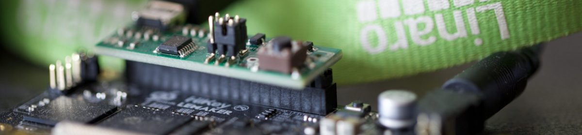
The ARMv8 architecture extends the AArch64 and AArch32 instruction sets with dedicated instructions for AES encryption, SHA-1 and SHA-256 cryptographic hashing, and 64×64 to 128 polynomial multiplication, and implementations of the various algorithms that use these instructions have been added to the ARM and arm64 ports of the Linux kernel over the past couple of years. Given that my main focus is on enterprise class systems, which typically use high end SoCs, I have never felt the urge to spend too much time on accelerated implementations for systems that lack these optional instructions (although I did contribute a plain NEON version of AES in ECB/CBC/CTR/XTS modes back in 2013). Until recently, that is, when I received a Raspberry Pi 3 from my esteemed colleague Joakim Bech, the tech lead of the Linaro Security Working Group. This system is built around a Broadcom SoC containing 4 Cortex-A53 cores that lack the ARMv8 Crypto Extensions, and as it turns out, its AES performance was dreadful.

AES primer

The Advanced Encryption Standard (AES) is a variant of the Rijndael cipher with a fixed block size of 16 bytes, and supports key sizes of 16, 24 and 32 bytes, referred to as AES-128, AES-192 and AES-256, respectively. It consists of a sequence of rounds (10, 12, or 14 for the respective key sizes) that operate on a state that can be expressed in matrix notation as follows:

| a0, b0, c0, d0 |
| a1, b1, c1, d1 |
| a2, b2, c2, d2 |
| a3, b3, c3, d3 |

where each element represents one byte, in column major order (i.e., the elements are assigned from the input in the order a0, a1, a2, a3, b0, b1, etc)

Each round consists of a sequence of operations performed on the state, called AddRoundKey, SubBytes, ShiftRows and MixColumns. All rounds are identical, except for the last one, which omits the MixColumns operation, and performs a final AddRoundKey operation instead.

AddRoundKey

AES defines a key schedule generation algorithm, which turns the input key into a key schedule consisting of 11, 13 or 15 round keys (depending on key size), of 16 bytes each. The AddRoundKey operation simply xor’s the round key of the current round with the AES state, i.e.,

| a0 ^ rk0, b0 ^ rk4, c0 ^ rk8,  d0 ^ rk12 |
| a1 ^ rk1, b1 ^ rk5, c1 ^ rk9,  d1 ^ rk13 |
| a2 ^ rk2, b2 ^ rk6, c2 ^ rk10, d2 ^ rk14 |
| a3 ^ rk3, b3 ^ rk7, c3 ^ rk11, d3 ^ rk15 |

where rkN refers to byte N of the round key of the current round.

SubBytes

The SubBytes operation is a byte wise substitution, using one of two S-boxes defined by AES, one for encryption and one for decryption. It simply maps each possible 8-bit value onto another 8-bit value, like below

| sub(a0), sub(b0), sub(c0), sub(d0) |
| sub(a1), sub(b1), sub(c1), sub(d1) |
| sub(a2), sub(b2), sub(c2), sub(d2) |
| sub(a3), sub(b3), sub(c3), sub(d3) |

ShiftRows

The ShiftRows operation is a transposition step, where all rows of the state except the first one are shifted left or right (for encryption or decryption, respectively), by 1, 2 or 3 positions (depending on the row). For encryption, it looks like this:

| a0, b0, c0, d0 |
| b1, c1, d1, a1 |
| c2, d2, a2, b2 |
| d3, a3, b3, c3 |

MixColumns

The MixColumns operation is also essentially a transposition step, but in a somewhat more complicated manner. It involves the following matrix multiplication, which is carried out in GF(28) using the characteristic polynomial 0x11b. (An excellent treatment of Galois fields can be found here.)

| 2, 3, 1, 1 |   | a0, b0, c0, d0 |
| 1, 2, 3, 1 |   | a1, b1, c1, d1 |
| 1, 1, 2, 3 | x | a2, b2, c2, d2 |
| 3, 1, 1, 2 |   | a3, b3, c3, d3 |

Table based AES

The MixColumns operation is computationally costly when executed sequentially, so it is typically implemented using lookup tables when coded in C. This turns the operation from a transposition into a substitution, which means it can be merged with the SubBytes operation. Even the ShiftRows operation can be folded in as well, resulting in the following transformation:

| 2, 3, 1, 1 |   | sub(a0), sub(b0), sub(c0), sub(d0) |
| 1, 2, 3, 1 |   | sub(b1), sub(c1), sub(d1), sub(a1) |
| 1, 1, 2, 3 | x | sub(c2), sub(d2), sub(a2), sub(b2) |
| 3, 1, 1, 2 |   | sub(d3), sub(a3), sub(b3), sub(c3) |

The generic AES implementation in the Linux kernel implements this by using 4 lookup tables of 256 32-bit words each, where each of those tables corresponds with a column in the matrix on the left, and each element N contains the product of that column with the vector { sub(N) }. (A separate set of 4 lookup tables based on the identity matrix is used in the last round, since it omits the MixColumns operation.)

The combined SubBytes/ShiftRows/MixColumns encryption operation can now be summarized as

| tbl0[a0]  tbl0[b0]  tbl0[c0]  tbl0[d0] |
|   (+)       (+)       (+)       (+)    |
| tbl1[b1]  tbl1[c1]  tbl1[d1]  tbl1[a1] |
|   (+)       (+)       (+)       (+)    |
| tbl2[c2]  tbl2[d2]  tbl2[a2]  tbl2[b2] |
|   (+)       (+)       (+)       (+)    |
| tbl3[d3]  tbl3[a3]  tbl3[b3]  tbl3[c3] |

where tblN refers to each of the lookup tables, (+) refers to exclusive-or, and the AES state columns are represented using 32-bit words.

Note that lookup table based AES is sensitive to cache timing attacks, due to the fact that the memory access pattern during the first round is strongly correlated with the key xor’ed with the plaintext, allowing an attacker to discover key bits if it can observe the cache latencies of the memory accesses.

Please refer to this link for more information about the AES algorithm.

Scalar AES for arm64

The first observation one can make when looking at the structure of the lookup tables is that the 4 tables are identical under rotation of each element by a constant. Since rotations are cheap on arm64, it makes sense to use only a single table, and derive the other values by rotation. Note that this does not reduce the number of lookups performed, but it does reduce the D-cache footprint by 75%.

So for the v4.11 release of the Linux kernel, a scalar implementation of AES has been queued for arm64 that uses just 4 of the the 16 lookup tables from the generic driver. On the Raspberry Pi 3, this code manages 31.8 cycles per byte (down from 34.5 cycles per byte for the generic code). However, this is still a far cry from the 12.9 cycles per byte measured on Cortex-A57 (down from 18.0 cycles per byte), so perhaps we can do better using the NEON. (Note that the dedicated AES instructions manage 0.9 cycles per byte on recent Cortex-A57 versions.)

Accelerated AES using the NEON

The AArch64 version of the NEON instruction set has one huge advantage over other SIMD implementations: it has 32 registers, each 128 bits wide. (Other SIMD ISAs typically have 16 such registers). This means we can load the entire AES S-box (256 bytes) into 16 SIMD registers, and still have plenty of registers left to perform the actual computation, where the tbl/tbx NEON instructions can be used to perform the S-box substitutions on all bytes of the AES state in parallel.

This does imply that we will not be able to implement the MixColumns operation using table lookups, and instead, we will need to perform the matrix multiplication in GF(28) explicitly. Fortunately, this is not as complicated as it sounds: with some shifting, masking and xor’ing, and using a table lookup (using a permute vector in v14) to perform the 32-bit rotation, we can perform the entire matrix multiplication in 9 NEON instructions. The SubBytes operation takes another 8 instructions, since we need to split the 256 byte S-box lookup into 4 separate tbl/tbx instructions. This gives us the following sequence for a single inner round of encryption, where the input AES state is in register v0. (See below for a breakdown of the MixColumns transformation)

/* AddRoundKey (round key pointer in x0) */
ld1	{v15.4s}, [x0], #16
eor	v0.16b, v0.16b, v15.16b

/* SubBytes (S-box in registers v16 - v31) */
movi	v15.16b, #0x40
sub	v9.16b, v0.16b, v15.16b
tbl	v0.16b, {v16.16b-v19.16b}, v0.16b
sub	v10.16b, v9.16b, v15.16b
tbx	v0.16b, {v20.16b-v23.16b}, v9.16b
sub	v11.16b, v10.16b, v15.16b
tbx	v0.16b, {v24.16b-v27.16b}, v10.16b
tbx	v0.16b, {v28.16b-v31.16b}, v11.16b

/* ShiftRows (permutation vector in v13) */
tbl	v0.16b, {v0.16b}, v13.16b

/* MixColumns (v12.16b = { 0x1b, 0x1b, ... }) */
sshr	v8.16b, v0.16b, #7
add	v9.16b, v0.16b, v0.16b
and	v8.16b, v8.16b, v12.16b
eor	v9.16b, v9.16b, v8.16b
rev32	v8.8h, v0.8h
eor	v8.16b, v8.16b, v9.16b
eor	v0.16b, v0.16b, v8.16b
tbl	v0.16b, {v0.16b}, v14.16b	/* ror	v0.4s, v0.4s, #8 */
eor	v0.16b, v0.16b, v8.16b

Looking at the instruction count, one would expect the performance of this algorithm to be around 15 cycles per byte when interleaved 2x or 4x (i.e., the code above, but operating on 2 or 4 AES states in parallel, to eliminate data dependencies between adjacent instructions). However, on the Raspberry Pi 3, this code manages only 22.0 cycles per byte, which is still a huge improvement over the scalar code, but not as fast as we had hoped. This is due to the micro-architectural properties of the tbl/tbx instructions, which take 4 cycles to complete on the Cortex-A53 when using the 4 register variant. And indeed, if we base the estimation on the cycle count, by taking 4 cycles for each such tbl/tbx instruction, and 1 cycle for all other instructions, we get the more realistic number of 21.25 cycles per byte.

As a bonus, this code is not vulnerable to cache timing attacks, given that the memory access patterns are not correlated with the input data or the key.

This code has been part of the arm64 Linux kernel since 2013, but some improvements to it have been queued for v4.11 as well.

Bit sliced AES using the NEON

The AES S-box is not an arbitrary bijective mapping, it has a carefully chosen structure, based again on finite field arithmetic. So rather than performing 16 lookups each round, it is possible to calculate the subsitution values, and one way to do this is described in the paper Faster and Timing-Attack Resistant AES-GCM by Emilia Kaesper and Peter Schwabe. It is based on bit slicing, which is a method to make hardware algorithms suitable for implementation in software. In the AES case, this involves bit slicing 8 blocks of input, i.e., collecting all bits N of each of the 128 bytes of input into NEON register qN. Subsequently, a sequence of logic operations is executed on those 8 AES states in parallel, which mimics the network of logic gates in a hardware implementation of the AES S-box. While software is usually orders of magnitude slower than hardware, the fact that the operations are performed on 128 bits at a time compensates for this.

An implementation of AES using bit slicing is queued for v4.11 as well, which manages 19.8 cycles per byte on the Raspberry Pi 3, which makes it the preferred option for parallelizable modes such as CTR or XTS. It is based on the ARM implementation, which I ported from OpenSSL to the kernel back in 2013, in collaboration with Andy Polyakov, who authored the ARM version of the code originally. However, it has been modified to reuse the key schedule generation routines of the generic AES code, and to use the same expanded key schedule both for encryption and decryption, which reduces the size of the per-key data structure by 1696 bytes.

The code can be found here.

Conclusion

For the Raspberry Pi 3 (as well as any other system using version r0p4 of the Cortex-A53), we can summarize the AES performance as follows:

AES performance (cycles per byte) CBC CTR XTS
encryption 24.7 19.8 20.1
decryption 22.2 19.8 22.7

Appendix: Breakdown of the MixColumns transform using NEON instructions

v0 =  |            a0,            b0,            c0,            d0 |
      |            a1,            b1,            c1,            d1 |
      |            a2,            b2,            c2,            d2 |
      |            a3,            b3,            c3,            d3 |

/* multiply by 'x' (0b10) in GF(2^8) */
sshr	v8.16b, v0.16b, #7
add	v9.16b, v0.16b, v0.16b
and	v8.16b, v8.16b, v12.16b
eor	v9.16b, v9.16b, v8.16b

v9 = |           2a0,           2b0,           2c0,           2d0 |
     |           2a1,           2b1,           2c1,           2d1 |
     |           2a2,           2b2,           2c2,           2d2 |
     |           2a3,           2b3,           2c3,           2d3 |

rev32	v8.8h, v0.8h

v8 = |            a2,            b2,            c2,            d2 |
     |            a3,            b3,            c3,            d3 |
     |            a0,            b0,            c0,            d0 |
     |            a1,            b1,            c1,            d1 |

eor	v8.16b, v8.16b, v9.16b

v8 = |        2a0^a2,        2b0^b2,        2c0^c2,        2d0^d2 |
     |        2a1^a3,        2b1^b3,        2c1^c3,        2d1^d3 |
     |        2a2^a0,        2b2^b0,        2c2^c0,        2d2^d0 |
     |        2a3^a1,        2b3^b1,        2c3^c1,        2d3^d1 |

eor	v0.16b, v0.16b, v8.16b

v0 = |        3a0^a2,        3b0^b2,        3c0^c2,        3d0^d2 |
     |        3a1^a3,        3b1^b3,        3c1^c3,        3d1^d3 |
     |        3a2^a0,        3b2^b0,        3c2^c0,        3d2^d0 |
     |        3a3^a1,        3b3^b1,        3c3^c1,        3d3^d1 |

tbl	v0.16b, {v0.16b}, v14.16b	/* ror	v0.4s, v0.4s, #8 */

v0 = |        3a1^a3,        3b1^b3,        3c1^c3,        3d1^d3 |
     |        3a2^a0,        3b2^b0,        3c2^c0,        3d2^d0 |
     |        3a3^a1,        3b3^b1,        3c3^c1,        3d3^d1 |
     |        3a0^a2,        3b0^b2,        3c0^c2,        3d0^d2 |

eor	v0.16b, v0.16b, v8.16b
  
v0 =  | 2a0^3a1^a2^a3, 2b0^3b1^b2^b3, 2c0^3c1^c2^c3, 2d0^3d1^d2^d3 |
      | 2a1^3a2^a3^a0, 2b1^3b2^b3^b0, 2c1^3c2^c3^c0, 2d1^3d2^d3^d0 |
      | 2a2^3a3^a0^a1, 2b2^3b3^b0^b1, 2c2^3c3^c0^c1, 2d2^3d3^d0^d1 |
      | 2a3^3a0^a1^a2, 2b3^3b0^b1^b2, 2c3^3c0^c1^c2, 2d3^3d0^d1^d2 |

Upstream support for AMD Overdrive in EDK2

Mainline EDK2 used to carry support for a number of ARM development platforms, such as TC2 and Juno (both of which are based on Versatile Express). These have been moved to OpenPlatformPkg, a separate platforms tree that is intended to complement the EDK2 mainline tree, and carries support for a number of platforms based on the ARM architecture (although non-ARM platforms are more than welcome as well).

Recently, EDK2 has gone back to only supporting various emulators (custom emulators built for Windows or X11, but also the QEMU system emulator in X86 or ARM mode) in its mainline tree, but the intention is to merge the entirety of OpenPlatformPkg back into EDK2 once a reorganization of the directory structure is completed. Until then, OpenPlatformPkg could be considered ‘upstream’ for all intents and purposes, as far as bare metal ARM platforms are concerned.

Upstream support for AMD Overdrive in EDK2

AMD is widely recognized for its efforts in open source, and as one of the founding members of the Linaro Enterprise Group (LEG), it has put its weight behind the work Linaro is doing to improve support for ARMv8 based servers in the enterprise.

As part of this effort, the UEFI engineers in LEG have been collaborating with AMD engineers to get support for AMD’s Overdrive platform into the EDK2 upstream. Due to its similarity to Overdrive, UEFI support for the upcoming LeMaker Celloboard is now public as well.

Special sauce

Unlike the Linux kernel community, which has a strict, GPL-based open source policy, the EDK2 community is lax about mixing open and closed source modules, and the fact that the EDK2 upstream by itself can only run on emulators attests to that. However, there is another way to combine the open source core components of EDK2 with closed source special sauce, by combining sources and binaries at the module level.

Binary modules in EDK2

The snippet below was taken from AmdSataInitLib.inf, showing how a static library that was built separately from the platform has been included as a binary module in the Overdrive build. The Binaries section appears instead of the usual Sources section, and contains the static library that makes up the module. (The .lib file in question was simply taken from a build that includes the module in source form, i.e., a .inf file containing the various sources in a Sources section, and a .dsc file that lists the .inf in a Components section.) The trailing asterisk means that the same file should be used for DEBUG and RELEASE builds.

[Binaries.AARCH64]
  LIB|AmdSataInit.lib|*


[FixedPcd]
gAmdModulePkgTokenSpaceGuid.PcdSATA0AlignPGen1
...

Note the FixedPcd section: a static EDK2 library will contain symbol references to the exact name/type combinations of these PCDs, and so it is recommended to use a strict match here (FixedPcd rather than Pcd)

In a similar way, complete PEI or DXE phase PE/COFF executables can be distributed in binary form as well, with the caveat that dynamic PCDs should be avoided (they simply don’t work)

Taking Gionb.inf as another example,

[Binaries.AARCH64]
  PE32|Gionb.efi|*
  PEI_DEPEX|Gionb.depex|*


[PatchPcd]
gAmdModulePkgTokenSpaceGuid.PcdPcieCoreConfiguration|2|0xa4d9
gAmdModulePkgTokenSpaceGuid.PcdPciePort0Present|1|0xa4c2
...

the first thing that stands out is the PEI_DEPEX line. The .depex file it refers to was taken from the same build that produced the .efi file, and is required by the runtime dispatcher to decide when the Gionb PEI module can be dispatched.

What is especially interesting about this module is the non-standard looking PCD references in the PatchPcd section. It lists the patchable PCDs that are referenced by the module, their default values, and their offsets into the binary (the .efi file from the Binaries section). If this module is incorporated into a platform .DSC that uses different values for these PCDs, the EDK2 build system will patch the desired values into a copy of the binary before incorporating it into the final firmware image. This is an especially powerful feature that allows us to share the Gionb module, which performs the PCIe link training, between the Overdrive and Cello platforms, which have different PCIe slot configurations.

In addition to AmdSataInitLib and Gionb, there are a few other modules that are distributed as binaries: IscpPei and IscpDxe, which produce the protocols to communicate with the SCP, and SnpDxePort0 and SnpDxePort1, which drive the two 10GigE ports.

Pre-UEFI firmware

The Overdrive platform is based on the AMD Seattle SOC, which combines a 32-bit ARM Cortex-A5 based System Control Processor (SCP) with up to 8 64-bit Cortex-A57 cores. The firmware that runs on the A5, and the secure world (EL3) firmware that runs on the A57s has not been published as source code, and is incorporated into the firmware image as a single binary blob. This means that only the code that executes in the same context as UEFI (EL2) has been released (modulo the binary modules mentioned above)

Call for collaboration

Apart from the pieces described above, the Overdrive UEFI firmware is completely open, and can be built and studied by anyone who is interested. This means anyone can upgrade their EDK2 core components if they want to enable things like new hardening features or HTTP boot. It also means people can contribute improvements and enhancements to the existing platform. One thing that is particularly high on my wish list is support for the Overdrive/Cello SD slot, which is simply an SD slot wired to an ARM standard PL022 SPI controller (and the Linux kernel already supports it). If anyone is interested in contributing that, please contact me with a proposal, and I will try to arrange support for it.